OUR MOTIVATION
The Task Group's M3 research contributes to PhoenixD's vision in particular through miniaturisation and integration. By combining different technologies, complex integrated optical systems are created.
Thin layer stacks of different materials are first deposited two-dimensionally on sacrificial substrates by advanced optical coating processes. They are then precisely diced by precision laser cutting und separated from the substrate. On the basis of this technology, free-standing microfilters with dimensions and thickness of a few 10 µm are produced. These substrate-free, miniaturized filters can take various functions in photonic circuits and belong to the key components of future photonic assembly techniques. For example, optical signals can be separated or combined with these filter components; also, more complex functions like distribution, filtering, or switching of light can be realised.
Embossing technology and injection moulding enable cost-efficient mass production of optics with spatially structured surfaces. Besides embossing techniques for the production of diffractive structures, injection moulding is applied by the working group to fabricate volume bodies with almost arbitrarily shaped but equally micro-structured surfaces.
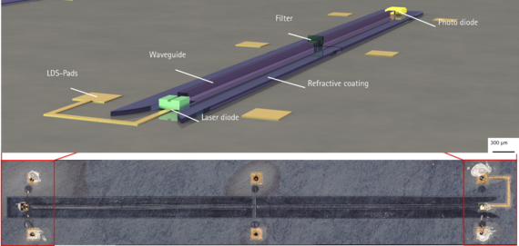
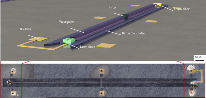
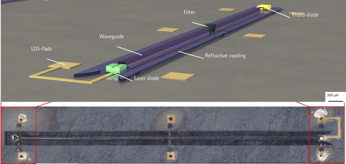
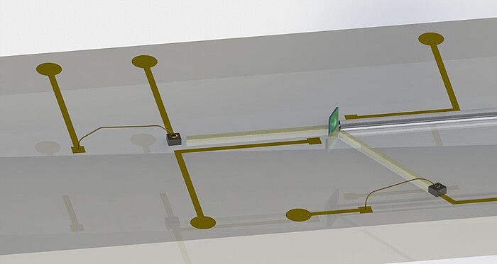
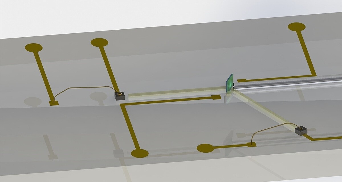
Especially, injection moulded optical carrier substrates, where optical micro components can be directly integrated, evolved from the working group. The optical connection is based on waveguides on the carrier substrate, and electrical contacting is achieved with printed or laser written conductor paths. The realisation of a first design with injection moulding on the way towards more complex systems involving also glass substrates is illustrated in figure 1.
 ©
Robin Basten/IMPT, Philipp Gehrke/LZH
Our Research
The basis for optical integration in the M3 working group is an optical platform (s. fig. 2), which is manufactured using precision injection moulding of polymer or alternatively fabricated on glass. The standard for fine structuring of the mould inserts for injection moulding is photolithography and electroplating. For the realisation on glass substrates additive manufacturing concepts and coating technologies with masking can be applied. Resolution in the range of micrometres can be achieved with these techniques, which is sufficient for passive waveguide structures.
For mounting and electrical contacting of active optical components such as light sources and detectors, the substrate has to be provided with electrical conductor paths. One possibility is metallic coating followed by lithographic patterning. Direct laser writing of conductor paths is an additive process for producing the electrical contacts on polyether ether ketone platforms.

 ©
Anna Karoline Rüßeler/LZH
The use of glass as a substrate material opens up additional degrees of freedom, in particular through precise surface quality with low roughness and flexible design options due to the high transparency in a wide wavelength range from the ultraviolet to the near infrared.
Optical gratings (s. fig. 3) are used, for example, in waveguides for coupling light in and out or in optical sensors. The structure sizes of such diffractive optical elements are well below one micrometre. Therefore, it is necessary to use electron-beam lithography, for example, to structure the mould inserts or the embossing stamps. As with injection moulding, the process technology for precision embossing of structures in the sub-micrometre range presents a significant challenge. To achieve consistent quality, one-off optimisation of the process parameters is not enough. Instead, manufacturing with adaptive process control in real-time is required.


 ©
Sebastian Bengsch/IMPT
Spectral filters and mirrors with dimensions in the micrometre range are essential for optical integration. The layer stacks are deposited in a coating chamber under vacuum in a batch process. The coatings are first produced over a large area and then divided into small platelets with high precision using a laser (s. fig. 4). These are now compatible with the Micro-Platform assembly process chain and can be fed in as components for example on releasable tape.


 ©
Anna Karoline Rüßeler/LZH
In addition to these passive layer systems, the working group also researches the development of active layers. The goal is optical filter coatings whose spectral characteristic that can be influenced by applying an electrical voltage during operation. For example, various optical signals can be decoupled from or fed into an optical data stream with such filters.
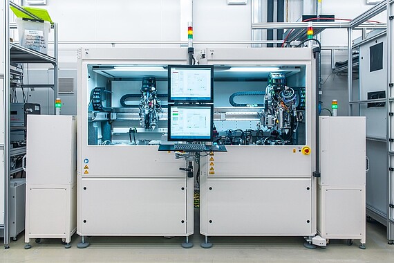
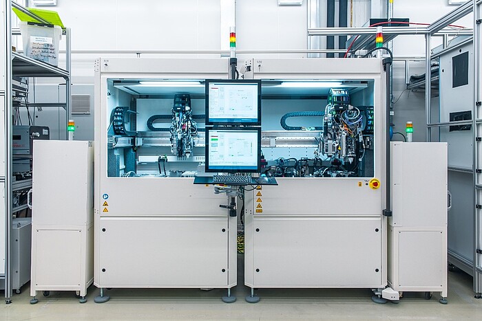
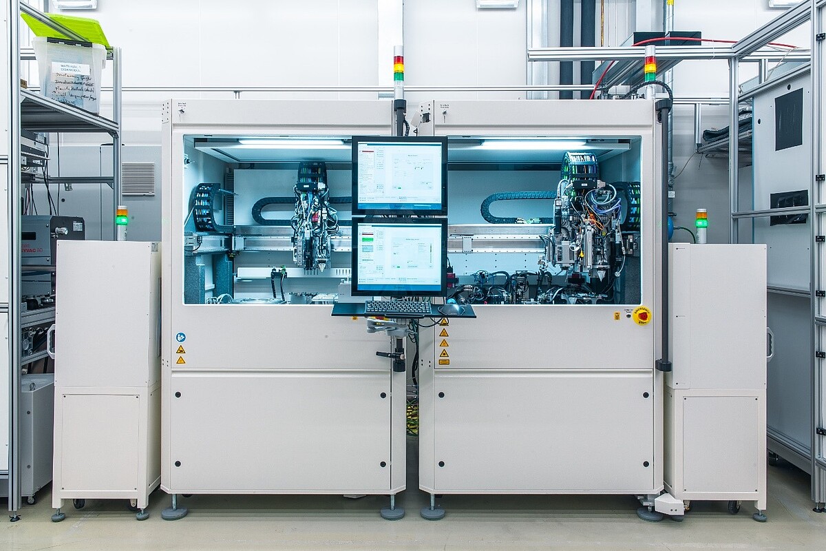
With a lift-off process, the delicate thin filter or mirror platelets can be detached from the substrate. In a unique custom pick-and-place system (s. fig. 5), the platelets are then inserted into the corresponding groves on the optical platform. Before fixing them, an individual active alignment procedure is implemented. For this purpose, the unique production facility can couple optical signals into the waveguides and monitor the signals.
 ©
Philipp Gehrke/LZH
The Task Group M3 collaborates in many ways with the other PhoenixD working groups. For example, there is an intensive cooperation with the researchers of the IHF – Institute for High-Frequency Technology – at TU Braunschweig and the Institute of Inorganic Chemistry at the Leibniz University Hannover to develop layered materials switching electro-optically. In this context, the Task Group jointly researches with the Task Group Optical Materials on modelling the corresponding layer structures. Scientists at the HOT – Hannover Centre for Optical Technologies – develop specific filter concepts to select optical signals in integrated optical systems. Besides, the Task Group investigates the coating of ultra-thin glass as an alternative process for the production of miniaturised thin-film filters for the work in Task Group Additive/Subtractive Manufacturing. There is close cooperation with the ITA – Institute of Transport and Automation Technology – in the field of bare die diodes. For example, the optical Micro-Platform utilises the ITA's high-precision wire bonding technology for the electrical contacting of the diodes used.
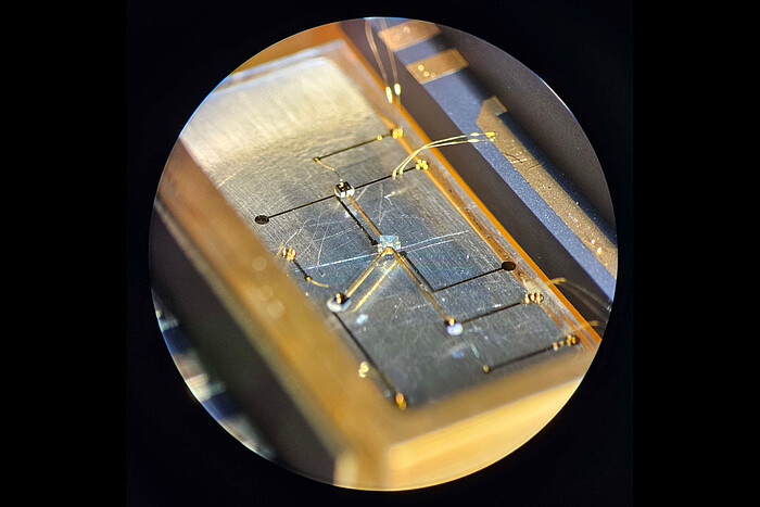
In figures 6 to 9 some recent examples for photonic assembly concepts developed within the co-operations are summarized. By now, free standing filters (s. fig. 6) can be integrated in conjunction with other components (s. fig. 7) and assembled to functional groups (s. fig. 8).


 ©
Philipp Gehrke/LZH


 ©
Philipp Gehrke, Anna Karoline Rüßeler/LZH

 ©
Birger Reitz/ITA
In cooperation with the working group of IHF of the TU Braunschweig, an electrically switching Fabry-Pérot structure could be realised by combination of two thin film reflectors. The switching function is achieved by a layer of amorphous polycarbonate which is doped with an electrically poled chromophore. This material reaches a very high electrooptical coefficient of up to 220 pm/V and in combination with the high field strengths in the layer structures enables a large switching dynamic. In figure 9, the integration of such a switch with two substrate-free reflectors in an optical circuit is depicted. The freestanding coating systems can be clearly identified, where the mirror with the switching coating exhibits a greenish surface.
Further targets of the working group concentrate on the production of more complex systems and the integration of additional optical elements. An accompanying focus is imposed on the testing of new concepts and optical materials for electrooptical switches on the basis of thin films.


 ©
Anna Karoline Rüßeler/LZH
Contact


30419 Hannover


